PSD
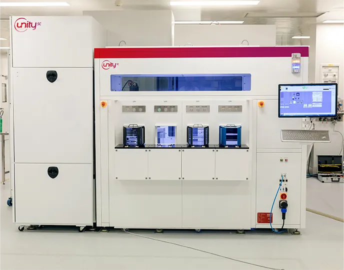
Metrology & Defect-Inspection combined systemIntroducing the PSD: Elevating Wafer Topography & Defect Control with Advanced Metro-Spection Technology
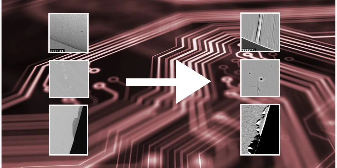
The PSD is a Phase-Shift-Deflectometry defect inspection tool, designed to catch ultra-low topography defects that DarkField and BrightField inspectors routinely miss.
This innovative tool doesn’t just spot defects, it also allows full wafer surface topography data collection. The PSD can be thought of as both Metrology and Inspection (Metro-Spection) combined.
Uniquely capable, the PSD performs simultaneous scans on both FrontSides and BackSides of wafers, at very high speeds, even on highly warped/bowed wafers, with very minimal edge-exclusion.
Beyond its prowess in inspecting unpatterned wafers, it is able to scan patterned wafers for Chip2Wafer-delamination, Wafer2Wafer-Delamination via buried-Voids, Film-delamination.
One of the standout features of the PSD is its resistance to surface noise, which can often impair DarkField inspections (particularly in the case of rough surfaces such as post-Silicon Grinding or SOI wafers). This makes the PSD an invaluable asset for inspecting post-Grind Silicon wafers, widely used in Silicon Power devices and other applications.
Furthermore, the PSD can share an EFEM with other UnitySC modules/tools, like the LightSpeed or an Edge inspection module, to form a cluster tool.
This integration not only reduces costs but also ensures a seamless, compromise-free implementation of 2 distinct Physics-based techniques. This combination is essential for detecting a diverse range of issues effectively.

Exploring PSD Key Use-Cases
Accommodating a variety of wafer types: suitable for both Opaque and Transparent Single Wafers, as well as Multi-Wafer Stacks:
- 1x Silicon wafer (including Pre/Post Backside Grind)
- Thin and Taiko wafers
- 1x Compound Semi Wafer (Low Topo Defects)
- 2x Bonded Wafers (e.g. Si-to-Si, to replace/complement C-SAM inspections)
- Chip2Wafer stacks (e.g. Find tiny degrees of delamination of Chips)
Use-Cases / Industry Segments include:
- Power Si Wafers
- MEMS Si wafers
- Glass Wafers (for Advanced Packaging)
- Compound wafers (all types)
- Wafer makers OQC
- Chip makers IQC
and more…

