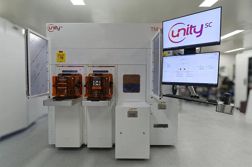
TMAP PLATFORM
Tailored Metrology Automated PlatformRevolutionizing Precision: Tailored, Automated and Future-Ready for Manufacturing Excellence
Our cutting-edge Metrology Platform, TMAP, is a revolutionary solution designed for precision and adaptability.
The TMAP comprises of a range of multiple non-contact modules, this platform can be tailored to meet your specific requirements.
Its fully automated handling (EFEM) makes TMAP a suitable tool from R&D to High Volume Manufacturing use cases, ensuring efficiency at every stage.
Ideal for both Front End and Back End of the line processes, our TMAP platform redefines industry standards, offering unparalleled accuracy and reliability for a future-ready manufacturing experience.

Exploring TMAP Key Use-Cases
- TSV / Depths & Diameters measurement, including HAR, TSVs as 3D IC, High BandWidth Memory (HBM) and SOIC
- Trench / Depths & CD measurement including HAR Trenches
- Redistribution Layers / Height & CD measurement
- Hybrid-Bonding W2W (WAFERtoWAFER), D2D (DIEtoDIE), D2W (DIEtoWAFER) / Cu dishing control (can be used together with the PSD tool for optimum sampling)
- Total Thickness Variation (TTV), including for materials such as Silicon that are opaque for Visible light

- Layer Thickness Variation (LTV) / Thin Film thickness measurements
- Bow/Warp measurement, for wafers of various material types
- Surface topography & CD measurements (Full Wafer and/or Local-topo at high XY resolution, Bump & Nail shape, roughness)
- W2W D2W Bonding / Overlay
- Stress measurements
- Edge-Trim metrology
- MEMS measurements
…and more, please contact us to discuss your specific requirements.

